- 您现在的位置:买卖IC网 > Sheet目录1971 > UPD78F1168AGF-GAS-AX (Renesas Electronics America)MCU 16BIT 78K0R/KX3 100-LQFP
CHAPTER 4 PORT FUNCTIONS
User’s Manual U17894EJ9V0UD
108
4.2.1 Port 0
Port 0 is a 7-bit I/O port with an output latch. Port 0 can be set to the input mode or output mode in 1-bit units
using port mode register 0 (PM0). When the P00 to P06 pins are used as an input port, use of an on-chip pull-up
resistor can be specified in 1-bit units by pull-up resistor option register 0 (PU0).
Input to the P03 and P04 pins can be specified through a normal input buffer or a TTL input buffer in 1-bit units
using port input mode register 0 (PIM0).
Output from the P02 to P04 pins can be specified as N-ch open-drain output (VDD tolerance) in 1-bit units using
port output mode register 0 (POM0).
This port can also be used for timer I/O, serial interface data I/O, clock I/O, internal system clock output, and
external wait signal input.
Reset signal generation sets port 0 to input mode.
Figures 4-2 to 4-7 show block diagrams of port 0.
Cautions 1. To use P01/TO00 as a general-purpose port, set bit 0 (TO00) of timer output register 0 (TO0)
and bit 0 (TOE00) of timer output enable register 0 (TOE0) to “0”, which is the same as their
default status setting.
2. To use P02/SO10/TxD1, P03/SI10/RxD1/SDA10, or P04/SCK10/SCL10 as a general-purpose
port, note the serial array unit 0 setting. For details, refer to the following tables.
Table 13-7 Relationship Between Register Settings and Pins (Channel 2 of Unit 0: CSI10,
UART1 Transmission, IIC10)
Table 13-8 Relationship Between Register Settings and Pins (Channel 3 of Unit 0: UART1
Reception)
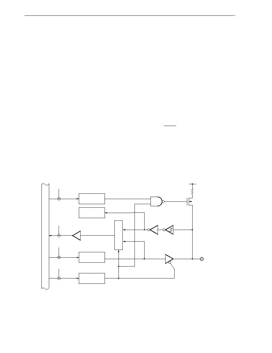
Figure 4-2. Block Diagram of P00
P00/TI00
WRPU
RD
WRPORT
WRPM
PU00
Alternate
function
Output latch
(P00)
PM00
EVDD0, EVDD1
P-ch
Selector
Internal
bus
PU0
PM0
P0
P0:
Port register 0
PU0:
Pull-up resistor option register 0
PM0:
Port mode register 0
RD:
Read signal
WR
××: Write signal
发布紧急采购,3分钟左右您将得到回复。
相关PDF资料
UPD78F1178AGF-GAT-AX
MCU 16BIT 78K0R/KX3 128-LQFP
UPD78F1188AGJ-GAE-AX
MCU 16BIT 78K0R/KX3 144-LQFP
UPD78F1235GK-GAJ-AX
MCU 16BIT 78K0R/LX3 64-LQFP
UPD78F4225YGC-8BT-A
MCU 16BIT 128K FLASH
UPD78F9202MA-CAC-A
MCU 8BIT 4KB FLASH 128B RAM
UPD78F9212CS-CAB-A
MCU 8BIT 4KB FLASH 16PIN
UPD78F9222CS-CAC-A
MCU 8BIT 4KB FLASH 20PIN
UPD78F9234CS-CAA-A
MCU 8BIT 8KB FLASH 30PIN
相关代理商/技术参数
UPD78F1168GC-UEU-AX
制造商:Renesas Electronics Corporation 功能描述:
UPD78F1168GF-GAS-AX
制造商:Renesas Electronics Corporation 功能描述:
UPD78F1174AGF-GAT-AX
功能描述:MCU 16BIT 78K0R/KX3 128-LQFP RoHS:是 类别:集成电路 (IC) >> 嵌入式 - 微控制器, 系列:78K0R/Kx3 标准包装:250 系列:80C 核心处理器:8051 芯体尺寸:8-位 速度:16MHz 连通性:EBI/EMI,I²C,UART/USART 外围设备:POR,PWM,WDT 输入/输出数:40 程序存储器容量:- 程序存储器类型:ROMless EEPROM 大小:- RAM 容量:256 x 8 电压 - 电源 (Vcc/Vdd):4.5 V ~ 5.5 V 数据转换器:A/D 8x10b 振荡器型:内部 工作温度:-40°C ~ 85°C 封装/外壳:68-LCC(J 形引线) 包装:带卷 (TR)
UPD78F1174GF-GAT-AX
制造商:Renesas Electronics Corporation 功能描述:
UPD78F1175AGF-GAT-AX
功能描述:MCU 16BIT 78K0R/KX3 128-LQFP RoHS:是 类别:集成电路 (IC) >> 嵌入式 - 微控制器, 系列:78K0R/Kx3 标准包装:250 系列:80C 核心处理器:8051 芯体尺寸:8-位 速度:16MHz 连通性:EBI/EMI,I²C,UART/USART 外围设备:POR,PWM,WDT 输入/输出数:40 程序存储器容量:- 程序存储器类型:ROMless EEPROM 大小:- RAM 容量:256 x 8 电压 - 电源 (Vcc/Vdd):4.5 V ~ 5.5 V 数据转换器:A/D 8x10b 振荡器型:内部 工作温度:-40°C ~ 85°C 封装/外壳:68-LCC(J 形引线) 包装:带卷 (TR)
UPD78F1176AGF-GAT-AX
功能描述:MCU 16BIT 78K0R/KX3 128-LQFP RoHS:是 类别:集成电路 (IC) >> 嵌入式 - 微控制器, 系列:78K0R/Kx3 标准包装:250 系列:80C 核心处理器:8051 芯体尺寸:8-位 速度:16MHz 连通性:EBI/EMI,I²C,UART/USART 外围设备:POR,PWM,WDT 输入/输出数:40 程序存储器容量:- 程序存储器类型:ROMless EEPROM 大小:- RAM 容量:256 x 8 电压 - 电源 (Vcc/Vdd):4.5 V ~ 5.5 V 数据转换器:A/D 8x10b 振荡器型:内部 工作温度:-40°C ~ 85°C 封装/外壳:68-LCC(J 形引线) 包装:带卷 (TR)
UPD78F1177AGF-GAT-AX
功能描述:MCU 16BIT 78K0R/KX3 128-LQFP RoHS:是 类别:集成电路 (IC) >> 嵌入式 - 微控制器, 系列:78K0R/Kx3 标准包装:250 系列:80C 核心处理器:8051 芯体尺寸:8-位 速度:16MHz 连通性:EBI/EMI,I²C,UART/USART 外围设备:POR,PWM,WDT 输入/输出数:40 程序存储器容量:- 程序存储器类型:ROMless EEPROM 大小:- RAM 容量:256 x 8 电压 - 电源 (Vcc/Vdd):4.5 V ~ 5.5 V 数据转换器:A/D 8x10b 振荡器型:内部 工作温度:-40°C ~ 85°C 封装/外壳:68-LCC(J 形引线) 包装:带卷 (TR)
UPD78F1177AGF-GAT-E2-AX
制造商:Renesas Electronics Corporation 功能描述: